Implementing a Game Boy emulator
Write-up about Play Kid, my own homegrown Game Boy emulator.
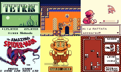
0.1.0, which works with SDL2. Since then, version 0.2.0 has been released. This new version uses Rust native crates like winit, egui, rodio, and pixels. See this write-up for more information on the new version.When I was a kid my parents got me and my brothers a brand new Game Boy. I used to play it a lot, and I was mesmerized and amazed at how such a tiny brick could give life to so many wonderful worlds. Some of my favorite games were Super Mario Land (1, 2, and 3, Wario Land), The Amazing Spider-Man, and Kirby’s Dream Land. We also had some other games, like Bugs Bunny Crazy Castle or Tetris, that I also played quite a lot. I remember fondly too.
The first Super Mario Land in particular was magical to me. I would complete it, and then do it again in one sitting. There were no save games, as it used MBC1 with no RAM (more on that later). You really had to git gud. The second play through had the same levels but more enemies, in what must have been one of the first implementations of New Game+. After this harder mode was completed, you could select and play any level. Too bad all the progress went away as soon as you powered off the device. Super Mario Land 2: 6 Golden Coins already introduced save games (used MBC1+RAM+Battery). It was a huge step-up in QoL for Game Boy games. We also had the original NES, and later the SNES, but the Game Boy always remained that cozy little fun device that you could just pick up and play for a quick session. It was a significant part of my childhood.
Me playing Super Mario Land, levels 2 to 4, with my own emulator.
Some time ago, I wrote a CHIP-8 emulator in Rust, and found the experience very rewarding. The consensus online seems to be that the recommended next step, as far as emulator development goes, is the original Game Boy. I know that the internet is flooded with “Implementing a Game Boy emulator” kind of articles, and (judging by the GitHub counts) this is a very unoriginal project, but I still wanted to try my hand at it. So I took the bait and started working on it. Today, I’m excited to share my very own Game Boy emulator.
The original Game Boy, also referred to as DMG in nerdy spaces and released in 1989, is an excellent target for emulation. Its hardware is rather well-documented, its architecture is relatively simple compared to modern systems, yet it’s complex enough to present real challenges, which I for sure faced.
I called my implementation Play Kid. It is written in Rust and uses SDL2 for graphics, sound, and input. Here are the main features:
- All CPU instructions implemented.
- Full memory map implemented.
- Modes: ROM, MBC1, MBC2, MBC3.
- Audio is implemented, with 4 channels, envelopes, sweep, and stereo.
- Supports game controllers via SDL (also hot-plugging).
- Multiple color palettes.
- Save screenshot of current frame buffer.
- Respects 160:144 aspect ratio by letter-boxing.
- Debug mode:
- Step instruction.
- Step scanline.
- Pause/continue current execution.
- FPS counter.
- Displays internal state.
- Breakpoints.
- Uses own minimal UI library with horizontal/vertical layouts, labels, buttons, and text fields.
- Save RAM to
.savfiles to emulate the battery-backed SRAM. - Automatically adapts to multi-DPI setups by scaling the UI.
- Working games/roms:
- Passes
dmg-acid2 - Tetris
- Pokémon Red
- Super Mario Land
- Super Mario Land 2: 6 Golden Coins
- Super Mario Land 3: Wario Land
- Wario Land II
- Bugs Bunny Crazy Castle
- The Amazing Spider-Man
- Kirby’s Dream Land
- Dr. Mario
- Probably many more
- Passes
- Works on Linux, macOS, and Windows.
In this post, I navigate the general architecture of the Game Boy, emphasize interesting hardware quirks that made it a challenge to emulate properly, and present my implementation. I won’t go into too much detail, as I took care to make the code understandable and well-commented. In any case, for more details on a specific subject, you can refer to the code repository itself.
Foreword
I have based my implementation, mainly, on three resources:
- Pan Docs – possibly the best documentation on the Game Boy system out there.
- Game Boy CPU Manual – documents the Game Boy architecture in great detail.
- Instruction table – all 8-bit opcodes into a single table, complete with descriptions for each one of them. Very handy.
On certain occasions, I found some of the Opcode descriptions to be unclear or a bit ambiguous. In these cases, I referred to actual pre-existing implementations. By far, the implementation I liked the most is RBoy. It is a very compact and mostly uncommented Game Boy Color emulator, written in Rust. Most of the instructions are the same as in the Game Boy DMG, so it worked very well for me.
Game Boy essentials
Before we get into the details, let’s talk a bit about how the Game Boy actually works. Emulation is basically about mimicking hardware in software. We’re not just running Game Boy code, we’re simulating an entire machine cycle by cycle.

The original Nintendo Game Boy. Original by Evan-Amos.
The Game Boy’s execution model is pretty simple. The CPU has a 16-bit PC register that points to the next instruction in memory. Each cycle, it fetches the byte at that address, decodes it into an instruction, executes it, and increments the PC. Instructions are composed of opcode+operand, and can be one, two, or three bytes long. Each instruction takes a specific number of machine cycles (M-cycles) to complete, usually between 1 and 6. Since the CPU runs at around 4.19 MHz (master clock) and one M-cycle equals four clock cycles (T-cycles), timing is important.
The system uses memory-mapped I/O. This means hardware components like the display, audio, and input are accessed by reading and writing to specific memory addresses. Want to check if the A button is pressed? Read from address 0xFF00. Need to start a DMA transfer? Write to 0xFF46. This design makes the architecture simpler, but it also means that memory access can trigger all sorts of side effects, and you need to manage the mapping in your code.
Interrupts let hardware grab the CPU’s attention. When something happens (the display finishing a frame, or a timer overflow), the corresponding interrupt flag is set. If interrupts are enabled (via the IME flag), the CPU pauses what it’s doing, pushes the current PC onto the stack, and jumps to a predefined interrupt handler address. This lets games sync with hardware events instead of constantly checking for them.
The hardware components all move forward together based on the CPU’s cycle count. When the CPU executes a 4 M-cycle instruction, the PPU advances 16 T-cycles worth of scanline rendering, the APU moves its sound generation forward, and timers tick along. Everything runs in lockstep, which means accurate emulation needs cycle-level precision across all the different parts.
Understanding this basic execution model (fetch, decode, execute, repeat, with interrupts and memory-mapped hardware mixed in) is key before getting into the specifics. Each part of the system we’ll look at next works within this framework.
The CPU
The heart of the Game Boy is a modified Intel 8080/Zilog Z80 processor running at approximately 4.19 MHz. Nintendo’s custom chip, sometimes called the SM83 or LR35902, includes most Z80 instructions but removes some and adds a few Game Boy-specific ones.
The CPU features eight 8-bit registers (A, B, C, D, E, F, H, L) that can be paired into four 16-bit registers (AF, BC, DE, HL), plus a 16-bit SP and the aforementioned PC. The F register is special, as its four most significant bits hold flags that track the results of operations:
- Zero (Z)
- Subtraction (N)
- Half-Carry (H)
- Carry (C)
In my implementation, the CPU is contained in machine.rs, which contains the main components of the hardware (memory, registers, PPU, APU, etc.), controls the execution state (with debug), and implements the instructions.
/// # Machine
/// The machine contains the registers, the memory, and the display, and
/// controls the execution and CPU state. It also implements the CPU, which
/// decodes and executes instructions.
pub struct Machine<'a, 'b> {
    /// The registers.
    pub registers: Registers,
    /// The main memory.
    pub memory: Memory<'a>,
    /// The display.
    display: Display<'b>,
    /// The UI state.
    ui_state: Rc<RefCell<UIState>>,
    /// Interrupt master enable flag.
    ime: bool,
    /// EI operation is delayed by one instruction, so we use this counter.
    ei: u8,
    /// DI operation is delayed by one instruction, so we use this counter.
    di: u8,
    /// Flag that holds the running status.
    running: bool,
    /// CPU halted.
    halted: bool,
    /// T-states, basic unit of time, and 1:1 with the clock.
    t_cycles: u32,
    /// M-cycles, base unit for CPU instructions, and 1:4 with the clock.
    m_cycles: u32,
    /// The debug manager.
    debug: DebugManager,
    /// Print FPS every second.
    fps: bool,
    /// The event pump.
    event_pump: EventPump,
}
The registers are implemented in a struct, which is trivial:
/// # Registers
/// We have 7 1-bit registers (`a`, `b`, `c`, `d`, `e`, `h`, `l`),
/// which can be accessed individually, or together as 16 bits,
/// in the combinations `af`, `bc`, `de` and `hl`.
/// We also have the flags register, `f`, whose 4 most significant bits are the flags
/// zero `z`, subtraction `n`, half-carry `h` and carry `c`.
/// Additionally, we have two 16-bit special registers, the stack pointer `sp`, and
/// the program counter `pc`.
pub struct Registers {
    pub a: u8,
    pub b: u8,
    pub c: u8,
    pub d: u8,
    pub e: u8,
    /// Flags register.
    /// - Bit 7: `z`, zero flag
    /// - Bit 6: `n`, subtraction flag (BCD)
    /// - Bit 5: `h`, half-carry flag (BCD)
    /// - Bit 4: `c`, carry flag
    pub f: u8,
    pub h: u8,
    pub l: u8,
    /// Stack pointer register.
    pub sp: u16,
    /// Program counter register.
    pub pc: u16,
}
This struct is complented with handy methods to read and write the registers, either individually or as 16-bit combinations. As you can see, the code is very well documented.
The instructions live in an enum, as do their operands. The instructions enum contains the 256 8-bit instructions, and the 256 16-bit instructions prefixed by 0xCB.
/// # Instructions
/// This enum contains all supported instructions.
/// Instructions that can act with both r8 and r16 registers are first named
/// by default in their r8 version. The r16 versions add a `16` at the end of the name.
#[derive(Debug)]
pub enum Instruction {
    // NoOp.
    NOP(),
    // Stop.
    STOP(),
    // Halt.
    HALT(),

    // Jump HL.
    JPHL(),
    // Jump.
    JP(CC),
    // Relative jumps.
    JR(CC),

    // Push.
    PUSH(R16EXT),
    // Pop.
    POP(R16EXT),

    // Load.
    LD(R8),
    LDcp(R8, R8),
    LD16(R16),
    [...]
}

/// Enumerates the r8 registers.
#[derive(Debug)]
pub enum R8 {
    A,
    B,
    C,
    D,
    E,
    H,
    L,
    HL,
}

/// Enumerates the r16 registers.
#[derive(Debug)]
pub enum R16 {
    BC,
    DE,
    HL,
    SP,
}

/// Enumerates r16 registers for POP and PUSH, which contain AF.
#[derive(Debug)]
pub enum R16EXT {
    BC,
    DE,
    HL,
    AF,
}

/// Enumerates the R16 registers to be used in (some) load operations.
#[derive(Debug)]
pub enum R16LD {
    BC,
    DE,
    HLp,
    HLm,
    A8,
    C,
    A16,
}

/// Enumerates jump conditions, mostly flags.
#[derive(Debug)]
pub enum CC {
    NONE,
    NZ,
    Z,
    NC,
    C,
}

/// RST's target address, divided by 8.
#[derive(Debug)]
pub enum TGT3 {
    T0,
    T1,
    T2,
    T3,
    T4,
    T5,
    T6,
    T7,
}
And then, I have a from_byte(byte: u8) method that matches opcodes to their actual enum values:
impl Instruction {
    /// Construct an instruction from its byte representation.
    pub fn from_byte(byte: u8) -> Option<Instruction> {
        match byte {
            // NOP
            0x00 => Some(Instruction::NOP()),
            // STOP
            0x10 => Some(Instruction::STOP()),

            // LD (r16)
            0x01 => Some(Instruction::LD16(R16::BC)),
            0x11 => Some(Instruction::LD16(R16::DE)),
            0x21 => Some(Instruction::LD16(R16::HL)),
            0x31 => Some(Instruction::LD16(R16::SP)),

            [...]

            // Undocumented OPCODE
            _ => {
                println!(
                    "{}: Unimplemented instruction {:#02x}, treating as NOP",
                    "WARN".yellow(),
                    byte
                );
                Some(Instruction::NOP())
            }
        }
    }
I also have a from_byte_0xcb(byte: u8) method used in the actual implementation to decode the 16-bit opcodes.
Actually implementing the CPU meant building a match with cases for ever single one of the 512 instructions. Each instruction updates the PC, manipulates registers or memory, and sets flags according to specific rules. Some instructions were very straightforward to implement; others, like DAA, required careful consideration of edge cases and bit manipulation. The implementation structure is quite straightforward:
    /// Execute a single instruction, and returns the number of cycles it takes.
    fn execute(&mut self, run_instr: RunInstr, opcode: u8) -> u8 {
        // Actually execute the instruction.
        match run_instr.instr {
            // NOP: no operation.
            Instruction::NOP() => 1,
            // STOP
            Instruction::STOP() => {
                self.stop();
                1
            }
            // HALT
            Instruction::HALT() => {
                // HALT only halts if IME is enabled.
                if self.ime {
                    self.halt();
                }
                // Otherwise, HALT acts like NOP.
                1
            }

            // LD r16
            Instruction::LD16(r16) => match r16 {
                R16::BC => {
                    let nw = self.read16();
                    self.registers.set_bc(nw);
                    3
                }
                R16::DE => {
                    let nw = self.read16();
                    self.registers.set_de(nw);
                    3
                }
                R16::HL => {
                    let nw = self.read16();
                    self.registers.set_hl(nw);
                    3
                }
                R16::SP => {
                    self.registers.sp = self.read16();
                    3
                }
            },

            [...]

            // OPCODE 16-bit (0xCB).
            Instruction::OPCODE16() => {
                // Read next byte, construct instruction, execute 0xCB instruction.
                let opcode0xcb = self.read8();
                let instr0xcb = Instruction::from_byte_0xcb(opcode0xcb);
                let msg = format!("Incorrect 0xCB opcode: {:#04X}", opcode0xcb);
                self.execute_0xcb(instr0xcb.expect(&msg), opcode0xcb)
            }

            // Never should happen.
            _ => panic!("Instruction is not implemented: {:#04X}", opcode),
        }
    }
And, of course, there is an analogous execute_0xcb(...) method that contains the implementation for all the 16-bit opcodes.
The CPU doesn’t run in isolation and needs to be cycle-accurate. Each instruction takes a specific number of machine cycles (M-cycles), typically 1-6, and the rest of the system needs to advance accordingly. Getting timing right is quite important, because the graphics hardware, audio, and even some games depend on precise cycle counts. This is why execute(...) -> u8 returns an unsigned integer. This is the number of cycles that the instruction takes. The main loop handles the input events, and then runs as many cycles per frame as necessary.
        while self.running {
            let frame_start_time = std::time::Instant::now();

            // Handle input events.
            self.handle_events();

            let mut cycles_this_frame: usize = 0;
            while cycles_this_frame < constants::CYCLES_PER_FRAME {
                let (t, m) = self.machine_cycle();
                self.m_cycles += m;
                self.t_cycles += t;
                cycles_this_frame += t as usize;

                // Fill the LCD buffer if needed.
                self.display.render_lcd(&mut self.memory);
            }

            // Flush and present the frame.
            self.display.canvas.flush();
            self.display.present();

            frame_count += 1;

            // Sleep for the remaining time in the frame.
            self.sleep_next_frame(frame_start_time);
        }
    }
The machine cycle runs a single CPU cycle. A CPU cycle does the following:
- Read next opcode from the memory address pointed by PC
- Increment PC
- Decode the instruction
- Run the instruction –
execute(...) - Run a memory cycle
- Update the IME and handle interrupts
The code looks like this:
    /// Main loop of the machine.
    fn cycle(&mut self) -> u8 {
        // Fetch next instruction, and parse it.
        let opcode = self.read8();
        let run_instr = RunInstr::new(opcode, &self.memory, &self.registers);

        // Execute the instruction.
        self.execute(run_instr, opcode)
    }

    /// Run a machine cycle.
    fn machine_cycle(&mut self) -> (u32, u32, bool) {
        // CPU instruction.
        // One machine cycle (M-cycle) is 4 clock cycles.
        let mut m_cycles = if self.running {
            if self.halted {
                // CPU is halted, don't execute instructions but still consume 1 M-cycle.
                1
            } else {
                // Run next CPU instruction.
                self.cycle() as u32
            }
        } else {
            // NOOP instruction.
            1
        };
        let mut t_cycles = m_cycles * 4;

        // Memory cycle.
        if m_cycles > 0 {
            // Memory cycle.
            let (_, r) = self.memory.cycle(t_cycles);
            if !r {
                // Close down.
                self.running = false;
                return (0, 0, false);
            }
        } else {
            t_cycles = 0;
            m_cycles = 0;
        }

        // Update IME.
        self.ime_update();

        // Handle interrupts if necessary.
        let interrupt_m_cycles = self.interrupt_handling();

        // Return.
        if interrupt_m_cycles > 0 {
            (interrupt_m_cycles * 4, interrupt_m_cycles, true)
        } else {
            (t_cycles, m_cycles, true)
        }
    }
We’ll talk about the memory cycle when we reach the memory section. For now, let’s look at interrupts, as it was an interesting challenge. The Game Boy supports five interrupt types: V-Blank, LCD STAT, Timer, Serial, and Joypad. The CPU checks for pending interrupts after each instruction, and if interrupts are enabled and one is pending, it pushes the PC onto the stack and jumps to the corresponding interrupt vector. Implementing the IME flag and its one-instruction delay after the EI instruction was a subtle detail that broke several games until I got it right. This is handled in ime_update() and interrupt_handling():
    /// Updates the IME (Interrupt Master Enable) flag.
    /// This is necessary because the effect of the EI and DI instructions
    /// is delayed by one instruction.
    fn ime_update(&mut self) {
        self.di = match self.di {
            2 => 1,
            1 => {
                self.ime = false;
                0
            }
            _ => 0,
        };
        self.ei = match self.ei {
            2 => 1,
            1 => {
                self.ime = true;
                0
            }
            _ => 0,
        };
    }

    /// Interrupt handling. The IF bit corresponding to this interrupt, and the IME flag
    /// are reset by the CUP. IF acknowledges the interrupt, and IME prevents any other
    /// interrupts from being handled until re-enabled (with RETI).
    /// In this case, the corresponding interrupt handler is called by pushing the PC
    /// to the stack, and then setting it to the address of the interrupt handler.
    fn interrupt_handling(&mut self) -> u32 {
        let pending = self.memory.ie & self.memory.iff;

        // Wake from HALT if any interrupt is pending (even if IME is disabled).
        if pending != 0 {
            if self.halted {
                self.halted = false;
            }
        }

        // If no interrupts are pending OR IME is disabled, return.
        if !self.ime || pending == 0 {
            return 0;
        }

        // Reset IME.
        self.ime = false;

        // IE and IF have the following format:
        //
        // | 7  6  5 |    4   |    3   |   2   |   1  |    0   |
        // |    1    | Joypad | Serial | Timer |  LCD | VBlank |
        //
        for i in 0..5 {
            let bit = 1 << i;
            if pending & bit != 0 {
                self.memory.iff &= !bit;
                let pc = self.registers.pc;
                self.push_stack(pc);
                self.registers.pc = match bit {
                    0x01 => 0x0040,
                    0x02 => 0x0048,
                    0x04 => 0x0050,
                    0x08 => 0x0058,
                    0x10 => 0x0060,
                    _ => panic!("Unknown interrupt bit {}", bit),
                };
                break;
            }
        }

        5 // 5 M-cycles = 20 T-cycles
    }
Memory
The Game Boy’s 16-bit address space is divided into distinct regions, each serving a specific purpose:
0x0000-0x3FFF: ROM bank 0 (16 KB, fixed)0x4000-0x7FFF: ROM bank 1-N (16 KB, switchable via MBCs, more on that later)0x8000-0x9FFF: Video RAM (8 KB)0xA000-0xBFFF: External RAM (8 KB, cartridge)0xC000-0xDFFF: Work RAM (8 KB)0xE000-0xFDFF: Echo RAM (mirror of 0xC000-0xDDFF)0xFE00-0xFE9F: OAM (sprite data)0xFF00-0xFF7F: I/O registers0xFF80-0xFFFE: High RAM (127 bytes)0xFFFF: IE register
Implementing memory access required a dispatcher that routes reads and writes to the appropriate hardware component. Reading from VRAM accesses the PPU’s memory, writing to 0xFF00-0xFF7F triggers side effects in various subsystems, and accessing cartridge ROM or RAM goes through the mapper.
The memory struct contains the Work RAM, the High RAM, I/O registers, the IF and IE, a reference to the PPU, a reference to the APU, a reference to the cartridge, the timer, and the joypad.
/// # Memory
/// The Game Boy uses a 2-byte address space (0x0000 to 0xFFFF) to map the different
/// types of memory (RAM, VRAM, Cartridge memory, etc.)
pub struct Memory<'a> {
    /// Work RAM.
    pub wram: [u8; constants::WRAM_SIZE],
    // High RAM.
    pub hram: [u8; constants::HRAM_SIZE],
    // I/O registers.
    pub io: [u8; constants::IO_SIZE],
    // IF: interrupt flag.
    pub iff: u8,
    // IE flag: interrupt enable.
    pub ie: u8,
    // Cartridge reference.
    pub cart: &'a mut Cartridge,
    /// The PPU, Picture Processing Unit.
    pub ppu: PPU,
    /// The timer.
    pub timer: Timer,
    /// The joypad.
    pub joypad: Joypad,
    /// The APU, Audio Processing Unit.
    pub apu: APU,
}
The actual mapping is implemented in the read() and write() operations. The address is matched to the specific range in the address space and forwarded to the appropriate component. For instance, the read method:
    /// Read a byte of memory at the given `address`.
    pub fn read8(&self, address: u16) -> u8 {
        match address {
            0x0000..=0x3FFF => {
                // 16kB bank #0 (cartridge).
                self.cart.read(address)
            }
            0x4000..=0x7FFF => {
                // 16kB switchable ROM bank (cartridge).
                self.cart.read(address)
            }
            0x8000..=0x9FFF => {
                // VRAM.
                self.ppu.read(address)
            }
            0xA000..=0xBFFF => {
                // 8kB switchable RAM bank (cartridge).
                self.cart.read_ram(address)
            }
            [...]
        }
    }
Memory-mapped I/O registers control everything from LCD modes to audio channels. Some registers are read-only, some write-only, and some have bits that behave differently on read versus write. The DMA register at 0xFF46 is particularly interesting. Writing to it triggers a transfer of 160 bytes from ROM or RAM to OAM, during which the CPU should only access High RAM. Getting DMA timing correct was essential for sprite-heavy games.
The PPU
The Picture Processing Unit is what puts pixels on the screen. It generates a 160×144 display running at around 60 Hz. Getting it working meant understanding scanlines, timing, and how backgrounds, windows, and sprites all come together.
The PPU works one scanline at a time. Each scanline takes 456 T-cycles (dots), and a full frame has 154 scanlines: 144 visible ones and 10 during V-Blank. While rendering a scanline, the PPU goes through different modes:
- Mode 2 (OAM Search): Scanning which sprites will be visible on this scanline (80 dots)
- Mode 3 (Pixel Transfer): Actually drawing the pixels (variable, ~172 dots)
- Mode 0 (H-Blank): Horizontal blank, waiting for the scanline to finish (~204 dots)
- Mode 1 (V-Blank): Vertical blank, screen done rendering (10 scanlines × 456 dots)
During V-Blank, games usually update their state and prepare for the next frame. My implementation transitions between modes based on the current scanline and dot count:
let new_mode = if self.ly >= 144 {
    1 // VBlank.
} else {
    match self.fdot {
        0..=80 => 2,   // OAM Scan.
        81..=252 => 3, // Drawing.
        _ => 0,        // HBlank.
    }
};
The background is made up of 8x8 pixel tiles stored in VRAM. Each tile uses 2 bits per pixel, giving you four shades of gray (or colors if you apply a palette). There are two tile data areas (at 0x8000 and 0x8800) and two tile maps that tell you which tiles go where. The LCDC register controls which areas to use, and you can think of it as configuring how the PPU interprets the data in VRAM.
Fetching tile data means reading two bytes per tile row and combining them to get the color IDs:
let tile_addr = tile_addr_base + (line * 2);
let low_byte = self.read(tile_addr);
let high_byte = self.read(tile_addr + 1);

let mut pixels = [0u8; 8];
for i in 0..8 {
    let color_id = ((high_byte >> (7 - i)) & 0x1) << 1 | ((low_byte >> (7 - i)) & 0x1);
    pixels[i] = color_id;
}
Windows work similarly to backgrounds but ignore scrolling. They’re positioned absolutely on screen using WX and WY registers. My implementation tracks an internal window line counter (WLY) that only increments when the window actually renders on a scanline, which is important for games that turn the window on and off mid-frame.
Sprites (or objects) are 8x8 or 8x16 pixels that sit on top of the background. The OAM holds up to 40 sprite definitions, each with position, tile index, and attributes like palette selection, flip flags, and priority. The hardware can only show 10 sprites per scanline, and when more than 10 overlap, priority goes to sprites with lower X coordinates first, then lower OAM index:
// Game Boy priority: X asc, then OAM index asc.
sprites.sort_by(|a, b| {
    if a.x != b.x {
        a.x.cmp(&b.x)
    } else {
        a.oam_index.cmp(&b.oam_index)
    }
});
One of the trickier parts was getting sprite priority right. The priority bit in the sprite attributes controls whether a sprite appears above all background pixels or only above background color 0. I store the background color IDs in a separate buffer as I render the background, then check against those values when drawing sprites:
let bg_color_id = self.priorities[self.ly as usize * constants::DISPLAY_WIDTH + x_pos];

let obj_behind_bg = (sprite.attributes & 0x80) != 0;
let sprite_has_priority = if obj_behind_bg {
    // Priority bit set: only draw sprite over BG color 0.
    bg_color_id == 0
} else {
    // Priority bit clear: always draw sprite (over any BG color).
    true
};
This lets me respect the priority rules properly without having to re-read background data.
I cache tile data while rendering each scanline to avoid repeatedly decoding the same tiles. For backgrounds and windows, I cache up to 32 tiles (one row). For sprites, I use a HashMap keyed by tile ID, line number, and flip flags.
The PPU’s timing had to be cycle-accurate. Each frame needs exactly 70224 T-cycles (154 scanlines × 456 dots). The main loop advances the PPU by the number of cycles the CPU just executed, and the PPU updates its mode and LY register (current scanline) accordingly:
pub fn cycle(&mut self, t_cycles: u32) {
    if !self.is_ppu_enabled() {
        return;
    }

    self.fdot += t_cycles;

    // Update mode if it changed.
    if new_mode != self.mode {
        self.update_mode(new_mode);
    }

    // Handle transition to next scanline.
    if self.fdot >= 456 {
        self.fdot -= 456;
        self.ly = (self.ly + 1) % 154;
    }
}
Getting the timing right was kind of important because some games rely on precise V-Blank and H-Blank timing. Otherwise, you get visual glitches, and good luck debugging them.
In order to test my PPU implementation, I turned to the DMG Acid2 test. This is a rather exhaustive PPU test in the form of a ROM. If you see a happy face with HELLO WORLD! above, and dmg-acid2 by Matt Currie below, you’re good. In my case, the right chin was missing. I spent an ginormous amount of time trying to get it to render properly. This is what I was getting:
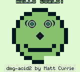
Oh no, the right chin is missing!
I was so close. The README has an entry that looks exactly like it. The right chin is rendered using the window, and the window tile map, so I kept looking at the window code. It was a pain, and for the life of me, I could not find the issue even though I looked incessantly. In the end, I fed my code to an LLM and it found the error right away: In my read and write VRAM operations, I had WX and WY backwards!
   // This is NOT correct!
   // WY.
   0xFF4A => self.wx,
   // WX.
   0xFF4B => self.wy,
This was frustrating, but it really goes to show what random side effects such a stupid mistake can have.
After countless hours, the stupid bug was mended and Acid2 was good!
Now that my PPU was more or less feature-complete, I tested it with other games. Seeing the first sprite render correctly, or watching the background scroll smoothly in Mario for the first time made it worth it. The PPU is obviously the most (only?) visible part of the emulator, so getting it to a state where it was able to run all the games I wanted to run felt good.
At the very end, when the graphics were already in an excellent shape, I implemented multiple color palettes. The original Game Boy was monochrome, but you can map those four gray shades to any colors you want. IIRC, the Super Game Boy did something similar, and it allowed you to create your own too! I included a few classic palettes (DMG Classic, Pocket, etc.) and some more creative ones. You can cycle through them while playing with p, which makes the games look fresh.
Some of the palettes in Play Kid.
At this point, I could play lots of games, but I had no audio. This had to be mended.
The APU
I consider the Audio Processing Unit (APU) to be one of the most boring parts of this project. It synthesizes sound through four channels: two pulse wave channels (square waves), one wave channel (custom waveform), and one noise channel (pseudo-random). Each channel has its own registers for frequency, volume, envelope, and duty cycle.
The APU is fully synchronized with the CPU and the PPU, and tus runs at 4.19 MHz. This is the master clock that we’ve seen previously. However, the APU doesn’t do everything at 4.19 MHz. Internally, it uses a frame sequencer that divides this master clock down to 512 Hz to manage high-level audio events:
- Length Counters: Clocked at 256 Hz (every 2nd step).
- Frequency Sweep: Clocked at 128 Hz (every 4th step).
- Volume Envelopes: Clocked at 64 Hz (every 8th step).
It steps through eight different phases, some updating length counters, some update the sweep function, and some updating volume envelopes. My implementation tracks this with a frame timer that increments with each T-cycle and runs at 512 Hz (4194304 Hz / 8192 = 512 Hz):
self.frame_timer += t_cycles;
if self.frame_timer >= 8192 {
    // 512Hz is 4.19 Mhz / 8192.
    self.frame_timer -= 8192;

    // Phases from 0 to 7.
    match self.frame_sequencer {
        0 | 2 | 4 | 6 => {
            self.step_length();
            if self.frame_sequencer == 2 || self.frame_sequencer == 6 {
                self.step_sweep();
            }
        }
        7 => {
            self.step_envelope_ch1();
            self.step_envelope_ch2();
            self.step_envelope_ch4();
        }
        _ => {}
    }
    self.frame_sequencer = (self.frame_sequencer + 1) % 8;
}
Each pulse channel (1 and 2) generates square waves with four different duty cycles. The duty cycle controls the waveform shape and is stored as patterns:
let duty_idx = (self.read(0xFF11) >> 6) as usize;
let patterns = [
    [0, 0, 0, 0, 0, 0, 0, 1],  // 12.5%
    [1, 0, 0, 0, 0, 0, 0, 1],  // 25%
    [1, 0, 0, 0, 0, 1, 1, 1],  // 50%
    [0, 1, 1, 1, 1, 1, 1, 0],  // 75%
];

let signal = patterns[duty_idx][self.ch1_duty_step];
let volume_multiplier = (self.ch1_volume as f32 / 15.0) * 0.05;
The wave channel (channel 3) is different. It plays back samples from a 32-nibble waveform stored in Wave RAM. Games can write custom waveforms here, which makes this channel super flexible:
// Get 4-bit sample from Wave RAM (32 samples total, 2 per byte).
let byte = self.wave_ram[self.ch3_sample_idx / 2];
let mut sample = if self.ch3_sample_idx % 2 == 0 {
    byte >> 4  // High nibble.
} else {
    byte & 0x0F  // Low nibble.
};

// Volume shift based on NR32 register.
sample >>= volume_shift;
The noise channel (channel 4) uses a LFSR to generate pseudo-random noise. The LFSR is a 15-bit shift register that XORs bits 0 and 1, then shifts the result back in:
let bit0 = self.ch4_lfsr & 0x01;
let bit1 = (self.ch4_lfsr >> 1) & 0x01;
let result = bit0 ^ bit1;

self.ch4_lfsr = (self.ch4_lfsr >> 1) | (result << 14);
if (nr43 & 0x08) != 0 {
    // Short mode (7-bit)
    self.ch4_lfsr = (self.ch4_lfsr & !(1 << 6)) | (result << 6);
}
This creates the characteristic noise used for drums, explosions, and other effects.
The sweep function on channel 1 was particularly tricky. It modulates the frequency over time by shifting the current frequency right and either adding or subtracting the result. The overflow check happens both when sweep is triggered and when calculating the new frequency:
fn calculate_sweep_freq(&mut self) -> u16 {
    let nr10 = self.read(0xFF10);
    let sweep_step = nr10 & 0x07;
    let descending = (nr10 & 0x08) != 0;

    let delta = self.ch1_sweep_shadow_freq >> sweep_step;
    let new_freq = if descending {
        self.ch1_sweep_shadow_freq.saturating_sub(delta)
    } else {
        self.ch1_sweep_shadow_freq + delta
    };

    // Overflow check.
    if new_freq > 2047 {
        self.ch1_enabled = false;
    }

    new_freq
}
Getting the timing and overflow behavior right required reading Pan Docs extensively, and I also looked at RBoy’s implementation.
Sound samples are generated at 44100 Hz and mixed into stereo output based on the NR51 register, which controls left/right panning for each channel. SDL2’s audio queue system fit naturally with the APU design. I generate samples as the emulator runs and queue them for SDL to play back:
let (l_sample, r_sample) = self.generate_sample();
self.buffer.push(l_sample);
self.buffer.push(r_sample);

if self.buffer.len() >= 2048 {
    // Throttle if queue is getting too full
    while self.device.size() > 8192 {
        std::thread::sleep(std::time::Duration::from_millis(1));
    }
    self.device.queue_audio(&self.buffer).unwrap();
    self.buffer.clear();
}
Keeping audio and video synchronized without drift required careful management of cycle counts and buffer sizes. The throttling mechanism prevents the emulator from running too fast when the audio queue backs up.
I implemented channel 1 first, and then ran Super Mario Land. I could hear some sounds (jumps, parts of the music), but the experience was underwhelming. Since all channels follow a similar structure, I had channel 2 working in no time. Now I could hear the iconic melody of the first stage, all the jumps, coins, and enemies. I implemented the other channels soon after.
Interestingly, in Super Mario Land, the music is mostly in channels 2 and 3. Channel 1 is for things like jumps, coins, and some high-pitched parts of melodies. Channel 4 is used in the random noise that some enemies produce when they die (like the bomb turtles), and some percussion beats in the background.
I still have no idea whether my APU contains any bugs, or if it sounds exactly as it’s supposed to. I have no way to tell. To my ears, it sounds amazing.
Cartridges
Most Game Boy cartridges aren’t just ROM chips. They contain MBCs that expand the addressable memory beyond the CPU’s 64 KB limit. Different games use different MBCs, each with its own banking scheme.
Every cartridge has a header header that contains essential information about the game, stored in the first few bytes of the cartridge’s ROM. This information helps the system identify and load the game properly. The header includes:
- Logo – the first 48 bytes (
0x00-0x2F) contain the Nintendo logo, ensuring the authenticity of the cartridge. - Title – the next 16 bytes (
0x34-0x43) store the 8-character game title, which is displayed when the game is loaded. - Game Boy/GBC Flag – the byte at
0x143indicates whether the game is for the original Game Boy (0x00), or a Game Boy Color-compatible game (0x80). - Cartridge Type – the byte at
0x147specifies the cartridge type, such as ROM-only or with memory banks. Here is a non-exhaustive list of common values:0x00– ROM only0x01– MBC10x02– MBC1+RAM0x03– MBC1+RAM+BATTERY0x05– MBC20x06– MBC2+BATTERY0x11– MBC30x12– MBC3+RAM0x13– MBC3+RAM+BATTERY
- ROM Size – the byte at
0x148specifies the ROM size in powers of 2. For example,0x00is 32KB,0x01is 64KB,0x02is 128KB, etc. - RAM Size – the byte at
0x149specifies the RAM size in kilobytes. For example,0x00means no RAM,0x03means 32KB,0x04means 128KB, etc. - Destination Code – located at
0x14A, this byte indicates the region the game is intended for.0x00is for Japan,0x01for Overseas. - Licensee Code – the byte at
0x14Bcontains a code identifying the licensed company that produced the game. - Mask ROM Version – the byte at
0x14Cis the version number of the game’s mask ROM (usually set to0x00). - Complement Checksum – the byte at
0x14Dis used for the checksum calculation to verify the integrity of the ROM data. - Global Checksum – the last 2 bytes (
0x14E-0x14F) store a checksum value that ensures the data integrity of the entire ROM.
This header allows the Game Boy to load and display the game properly by checking for compatibility and loading the correct resources for the specified hardware.
When it comes to MBCs, I implemented ROM-only and MBC1/2/3 into Play Kid.
- ROM-only
- ROM-only cartridges are the simplest, with no banking at all. These are limited to 32 KB and include simple games like Tetris. No mapper logic needed, just direct reads from the ROM data.
Tetris and Dr. Mario use ROM-only cartridges.
- MBC1
- MBC1 is the most common mapper, supporting up to 2 MB of ROM and 32 KB of RAM. It uses banking to switch between ROM and RAM banks by writing to specific address ranges. Understanding that writes to ROM addresses don’t actually write to ROM but instead configure the mapper took some mental adjustment.
MBC1 has two banking modes controlled by a mode register. In ROM banking mode (mode 0), you get access to more ROM banks but only one RAM bank. In RAM banking mode (mode 1), you can switch between multiple RAM banks but lose access to the upper ROM banks:
pub fn write(&mut self, address: u16, value: u8) {
    match address {
        // RAM enable.
        0x0000..=0x1FFF => {
            self.ram_enabled = (value & 0x0F) == 0x0A;
        }
        // ROM bank number (lower 5 bits).
        0x2000..=0x3FFF => {
            let mut bank = value as usize & 0x1F;
            if bank == 0 {
                bank = 1;  // Bank 0 becomes bank 1.
            }
            self.rom_bank = (self.rom_bank & 0x60) | bank;
        }
        // RAM bank or upper ROM bank bits.
        0x4000..=0x5FFF => {
            let bits = value as usize & 0x03;
            if self.banking_mode == 0 {
                self.rom_bank = (bits << 5) | (self.rom_bank & 0x1F);
            } else {
                self.ram_bank = bits;
            }
        }
        // Banking mode select.
        0x6000..=0x7FFF => {
            self.banking_mode = value & 0x01;
        }
        _ => {}
    }
}
Super Mario Land (1 and 2), Wario Land, Kirby’s Dream Land, and The Amazing Spider-Man all use MBC1.
- MBC2
- MBC2 has a quirky design. It includes 512×4 bits of built-in RAM, and bit 8 of the write address determines whether you’re configuring ROM banking or RAM enable. Both operations share the same address range (
0x0000-0x1FFF): match addr { 0x0000..=0x1FFF => { if (addr >> 8) & 0x01 == 0 { // Bit 8 is 0: RAM enable. self.ram_enabled = (val & 0x0F) == 0x0A; } else { // Bit 8 is 1: ROM bank select. self.rom_bank = val & 0x0F; if self.rom_bank == 0 { self.rom_bank = 1; } } } // ... }Since MBC2’s RAM is only 4 bits per byte, reads return the value OR’d with 0xF0, and writes mask to the lower 4 bits.
I think I have not tested any game that uses MBC2.
- MBC3
- MBC3 adds a real-time clock (RTC) alongside standard ROM/RAM banking. The RTC includes seconds, minutes, hours, and days counters that can be accessed by setting the RAM bank register to values
0x08-0x0C. I understand that some games use the RTC to track time-based events, but I have not tested this: pub fn read_ram(&self, address: u16) -> u8 { if !self.ram_enabled { return 0xFF; } match self.ram_bank { 0x00..=0x03 => { // Standard RAM banks. let offset = (self.ram_bank * 0x2000) + (address as usize - 0xA000); self.ram[offset % self.ram.len()] } 0x08 => self.rtc_seconds, 0x09 => self.rtc_minutes, 0x0A => self.rtc_hours, 0x0B => self.rtc_days_low, 0x0C => self.rtc_days_high, _ => 0xFF, } }The RTC is latched by writing 0 then 1 to address range
0x6000-0x7FFF. This copies the current time into the registers so the game can read a consistent value. My implementation updates the RTC with system time:fn update_rtc(&mut self) { let now = SystemTime::now() .duration_since(UNIX_EPOCH) .unwrap() .as_secs(); self.rtc_seconds = (now % 60) as u8; self.rtc_minutes = ((now / 60) % 60) as u8; self.rtc_hours = ((now / 3600) % 24) as u8; let days = (now / 86400) as u16; self.rtc_days_low = (days & 0xFF) as u8; // Day MSB and carry flag. let day_msb = ((days >> 8) & 0x01) as u8; self.rtc_days_high = (self.rtc_days_high & 0xFE) | day_msb; if days > 511 { self.rtc_days_high |= 0x80; // Set overflow flag. } }Pokémon and Wario Land II use MBC3.
Finally, I implemented battery-backed SRAM. It meant saving the contents of cartridge RAM to .sav files when the emulator exits and loading them on startup, if they exist. You can also trigger the save operation at any time with w. I get the RAM from the cartridge, and then persist it (if not empty):
    /// Save SRAM of current cartridge to `.sav` file.
    pub fn save_sram(&self, rom_path: &str) {
        let save_path = Path::new(rom_path).with_extension("sav");

        // Only save if the mapper actually has RAM.
        let ram_data = match &self.cart_type {
            CartridgeType::MBC1(mbc) => &mbc.get_ram(),
            CartridgeType::MBC2(mbc) => &mbc.get_ram(),
            CartridgeType::MBC3(mbc) => &mbc.get_ram(),
            _ => return,
        };

        if !ram_data.is_empty() || matches!(self.cart_type, CartridgeType::MBC2(_)) {
            if let Ok(mut file) = File::create(&save_path) {
                let _ = file.write_all(ram_data);
                println!(
                    "{}: Save data written to disk: {}",
                    "WR".magenta(),
                    save_path.display()
                );
            }
        }
    }
The load operation checks for the file, loads it if it exists, and passes it to each MBC’s set_ram() method.
This feature is essential for saving progress in many games. Currently, the .sav files are written to the same directory where the ROM file is, with the same name and sav extension.
UI and debug mode
In order to help me debug the emulator as development progressed, I implemented a terminal-based debug interface that let me look under the hood and inspect the internal state of the machine. This is implemented in the src/debugcli.rs file in the repository, but it is now unused.
When the emulator was already working quite well, I implemented a GUI debug mode with a custom immediate-mode UI library built on top of SDL2 rendering. You can enable it at any time with d.
The UI library supports horizontal and vertical layouts, labels, buttons, and text fields. Enough to build a useful debug interface without pulling in a fat dependency. It’s minimal but effective. Writing it was not trivial. I knew that UI libraries are complex and take a lot of work to get right, and this little spin-off sub-project only confirmed this knowledge.
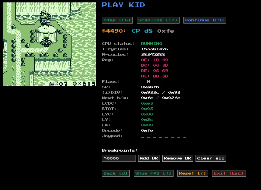
Super Mario Land 2 running in Play Kid with the debug UI.
The debug mode features:
- Current instruction, operand, and PC
- Opcode
- CPU status (either RUNNING or HALTED)
- M- and T-cycles
- CPU registers and flags
- PPU state (LCDC, STAT, LYC, LY, LX)
- Joypad state for all inputs (U, D, L, R, A, B, START, SELECT)
- Breakpoints
You can step through execution one instruction (F6) or one scanline (F7) at a time, pause and continue (F9), and set breakpoints at specific addresses. You can also reset the CPU with r. I also included an FPS counter (f). You can enable and disable the debug mode at any time with d.
One quality-of-life feature I’m proud of is automatic DPI scaling. On high-DPI displays, the UI scales appropriately so everything remains readable without manual configuration. This was a pain to handle manually. The emulator also respects the Game Boy’s 160:144 aspect ratio by letterboxing the display. It’s a small detail, but it ensures games look correct rather than stretched or squashed.
Future work
Here are some items I would like to do at some point:
- Move away from SDL2 in favor of Rust-native libraries like
winit+pixels+rodiofor easy cross-compilation, and web. I actually have a branch where I implemented the APU usingrodio - Implement more MBCs if I stumble upon games that need them.
- Add Game Boy Color support. As I understand it, it is not too complicated.
Conclusions
Building Play Kid taught me more about computer architecture, bit manipulation, and systems programming than any tutorial could. Every component of the Game Boy (CPU, memory, graphics, audio) works in concert, and understanding their interactions required patience, testing, and a lot of debugging.
Rust was an excellent choice for this project. My CHIP-8 emulator was already written in Rust, so this was a safe choice for me. I think the language has been praised enough at this time, so I’ll spare this part. SDL2 provided a simple, cross-platform foundation for rendering, input, and audio without unnecessary complexity.
If you’re interested in emulation, I think the Game Boy is a solid choice as first project if you have previous programming experience. The documentation is excellent and the hardware is approachable.